

by Mat Dirjish
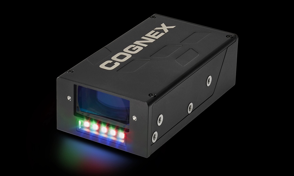
Machine vision tech company Cognex claims its In-Sight 1750, a next-generation wafer and panel identification system, will help semiconductor manufacturers reduce disruptions, improve traceability, and maintain throughput. The system reads many difficult wafer and panel markings and IDs, including various degraded marks and challenging substrates that often require intervention. It employs the company’s latest AI, imaging, and purpose-built illumination technologies to maintain traceability and throughput in challenging semiconductor environments.
Cognex points out several user benefits In-Sight 1750 offers. These include:
- Greater reliability of wafer traceability to maintain quality and process control throughout fabrication and packaging.
- Fewer production disruptions to reduce the need for operator intervention and manual troubleshooting.
- Faster upgrades, allowing existing users to transition from previous-generation systems without extensive redesign.
- Higher equipment utilization, helping manufacturers maintain throughput even when reading difficult marks on challenging wafer and substrate materials.
Additionally, the In-Sight 1750 system promises to fit seamlessly into existing operations and its new web-based setup simplifies configuration. For deeper details, procure and peruse the In-Sight 1750 datasheet.

